TLDR: Kate, a hardware security researcher, published a write-up on November 10 explaining how she turned two discontinued Nvidia CMP 170HX mining cards into devices that report 81,920 MiB of memory and outperform a retail A100 on FP16 throughput. It enables 80GB of accelerator memory for anyone willing to attack the card physically. The difference between this and the existing firmware method is the method: instead of rewriting firmware, she glitches the voltage supply to make the chip’s own fuses read as zero.
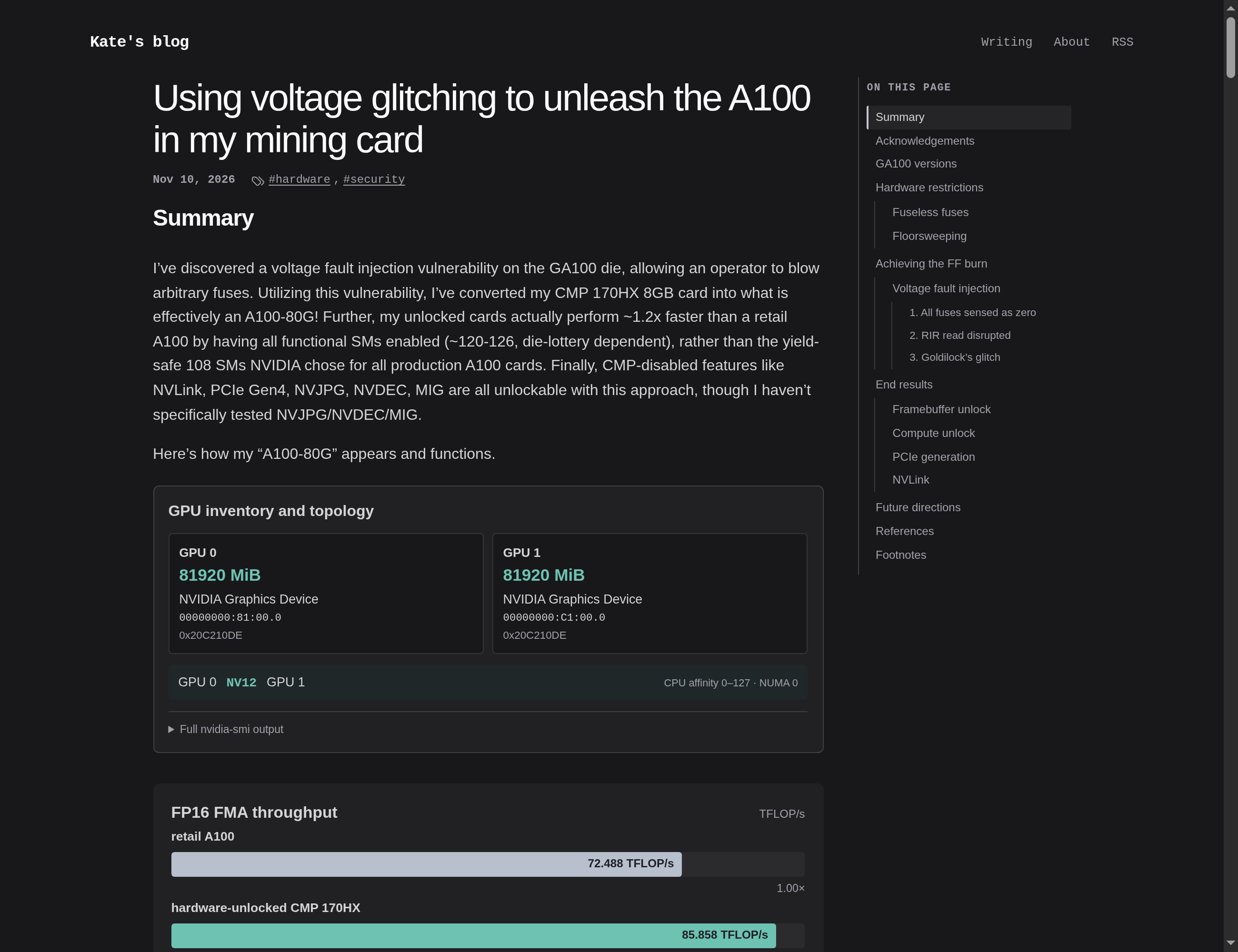
Caption: The post, which opens with an inventory showing two cards at 81,920 MiB each before explaining how they got there. Screenshot: blog.kate.land.
What the card is, and what was done to it
The CMP 170HX is a mining card built on the GA100 die, the same silicon as the A100, sold with most of its compute and memory disabled. Nvidia uses fuses to segment products: the chip ships with features physically switched off, not merely locked in software.
Kate’s approach is voltage fault injection. By disturbing the supply voltage at the right moment, the chip can be made to read its own fuse values as zero, which removes the restrictions rather than working around them. Her post walks through the sequence: getting all fuses sensed as zero, disrupting the RIR read, and finding what she calls “Goldilock’s glitch”, a window narrow enough to work reliably.
The result, on two cards:
- 81,920 MiB of framebuffer, reported by the driver
- 124 compute units at 1,410 MHz, against the 108 SMs Nvidia ships on retail A100s
- 85.858 FP16 TFLOPS, against 72.488 for a retail A100, about 18 percent more
- 1,883 GB/s coalesced read bandwidth, with writes at 2,137 GB/s
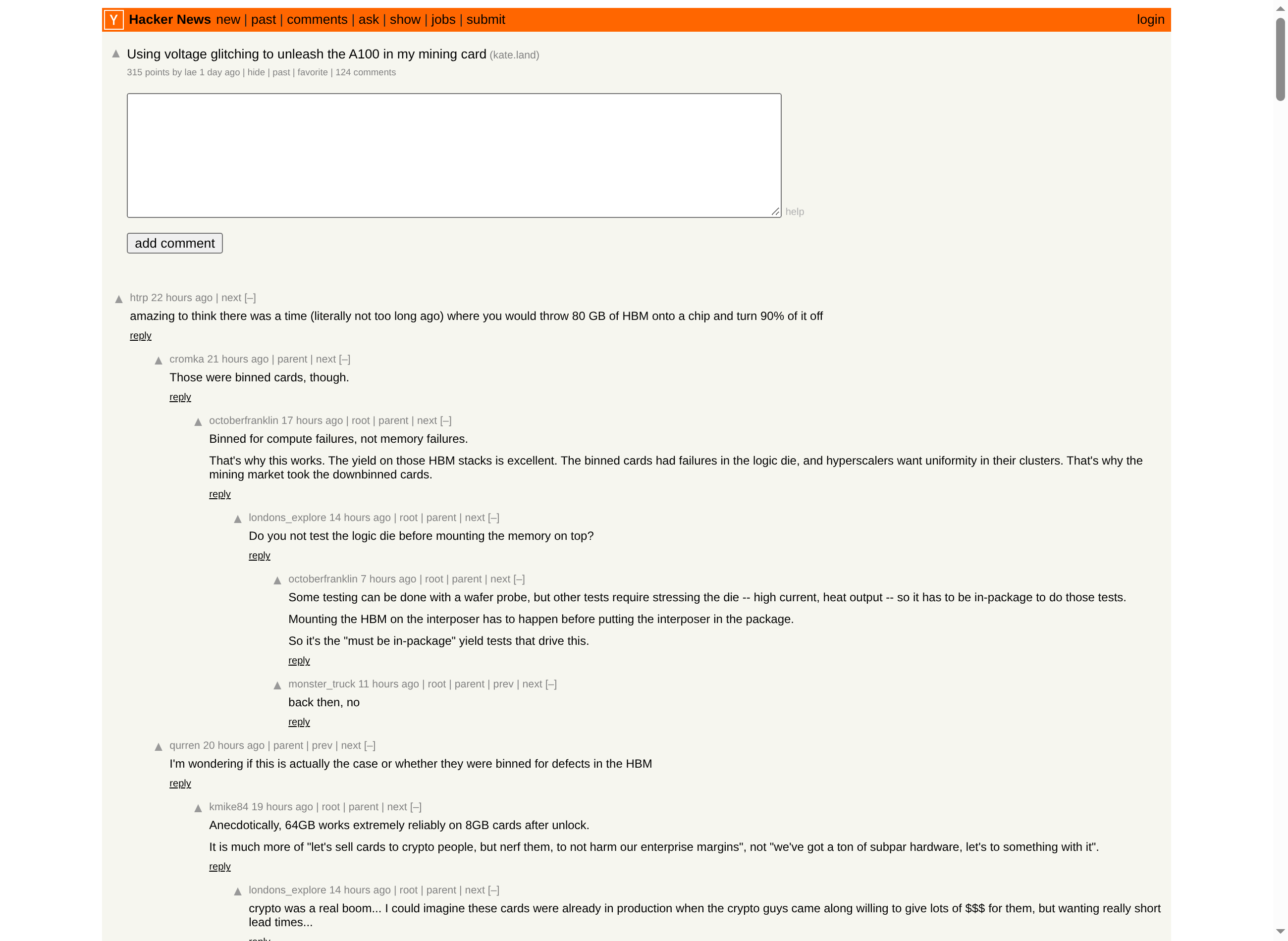
Caption: The discussion thread, where the arguments are about whether this is recovery or fraud, and how long the card will survive it. Screenshot: Hacker News.
The extra compute units come from the same place the extra memory does: Nvidia bins dies by yield, and a card sold as scrap may carry silicon that is more capable than the part number suggests. Enabling all of it is a lottery per die, which she says openly, quoting roughly 120 to 126 SMs depending on the chip.
The detail that keeps it honest
The post says PCIe Gen4 and NVLink can both be enabled with this approach. The same output shows the measured link at 11.58 GB/s bidirectional, labelled Gen3 x16.
That is not a contradiction so much as a limit of the test bench: the fuses governing the link can be relaxed, but the slot, riser and board still have to carry it. For anyone thinking about model serving, this matters more than the TFLOPS number, because a fast card behind a slow link spends its time waiting for the next batch of tokens.
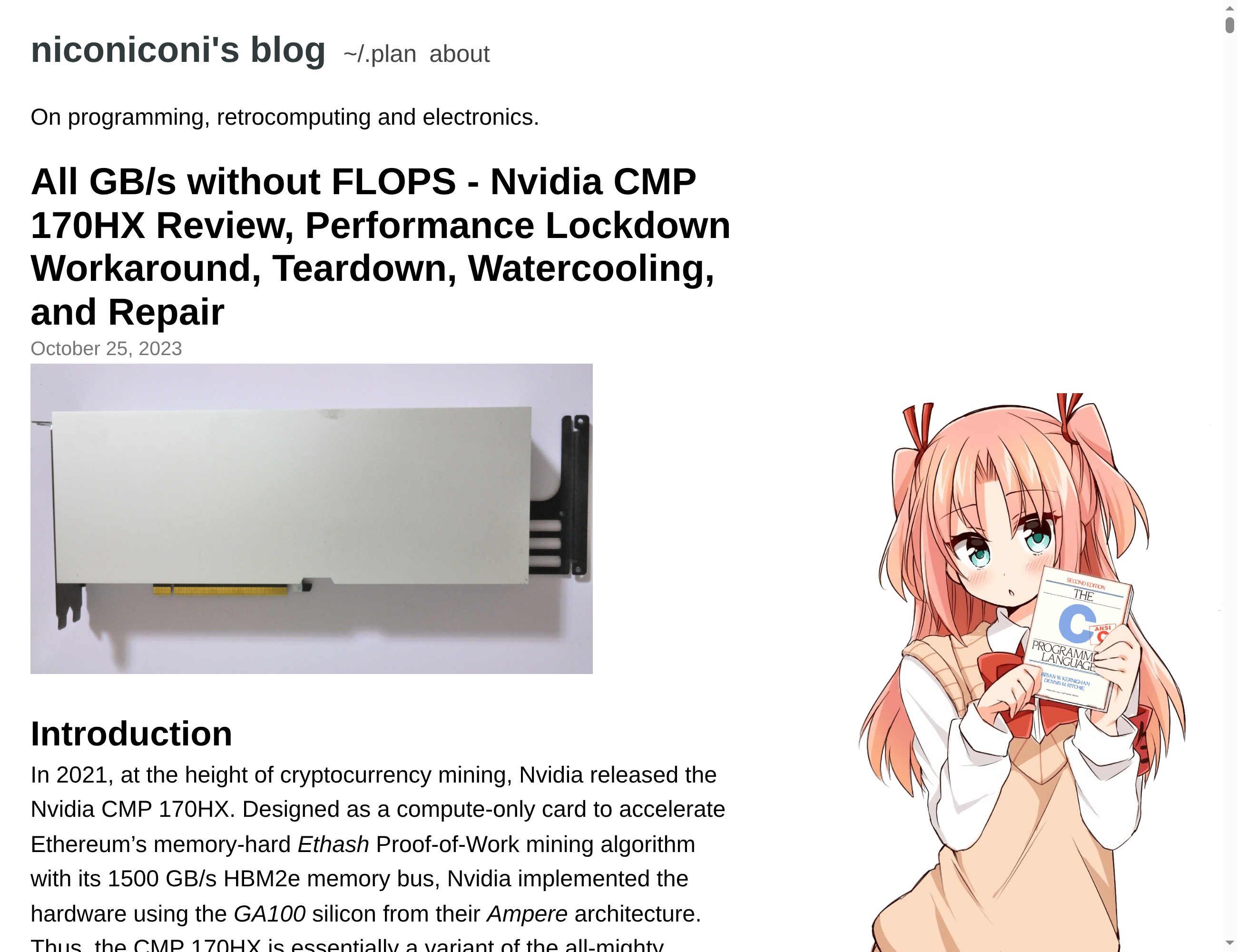
Caption: The hardware review that documented what the card was supposed to be: a deliberately crippled GA100 sold for mining, with bandwidth and compute both restricted. Screenshot: niconiconi.neocities.org.
This is not the first attempt
There is an established line of work here, and Kate’s post is one entry in it rather than a one-off.
A community project with a GPL licence, whose own summary is a tool to “unlobotomize your NVIDIA card,” has been on GitHub since July 2026 and has about 848 stars.
MRMCD 2026 hosted a talk titled “FACEB13D exploit: Liberating the A100 beast inside Nvidia’s CMP 170HX e-waste,” which describes recovering an AES key from a debug UEFI module to bring up 64 GB of HBM2e and around 200 TFLOPS of compute. A different route to a different, also enormous, result.
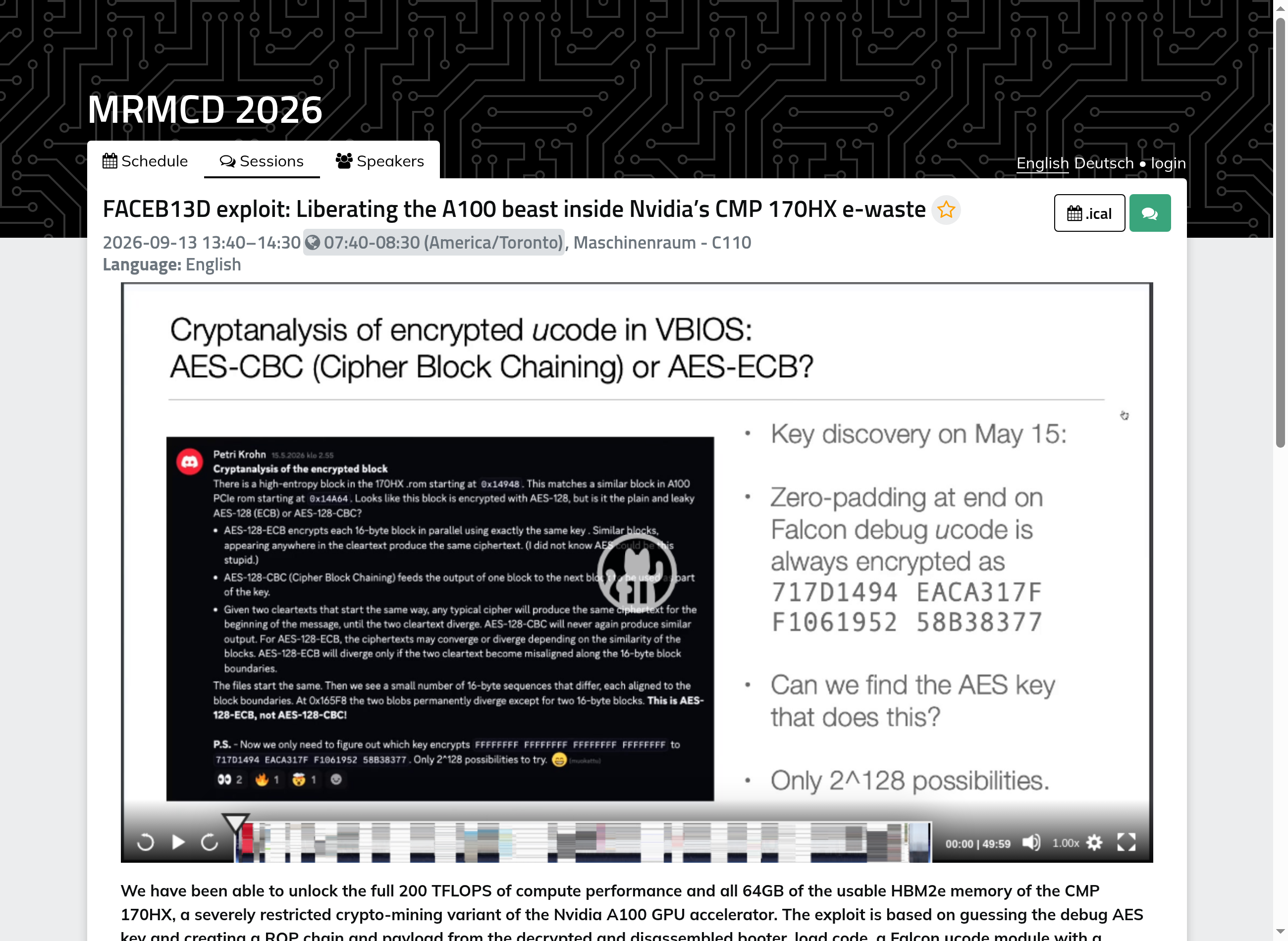
Caption: The conference talk, which attacked the same card through its BIOS rather than its power supply and reports a different ceiling: 64GB of HBM2e. Screenshot: MRMCD 2026.
Two methods, two ceilings, same die. That is worth knowing before treating any single number as “the” spec of a card after the procedure.
What it would mean if you could buy one
Eighty gigabytes of accelerator memory is more than two RTX 5090s, and the card it comes from was sold as e-waste. On paper that is the most interesting VRAM-per-dollar story in local AI since the 3090.
In practice there are four problems:
- The procedure is physical. It requires access to the card’s power delivery, instrumentation and patience. It is not a firmware flash.
- Every card is a lottery. SM counts and memory yield vary by die.
- Support is zero. No warranty, no vendor driver validation, and a card Nvidia never intended to sell for compute.
- The link is the bottleneck. 80GB is only useful if you can feed it.
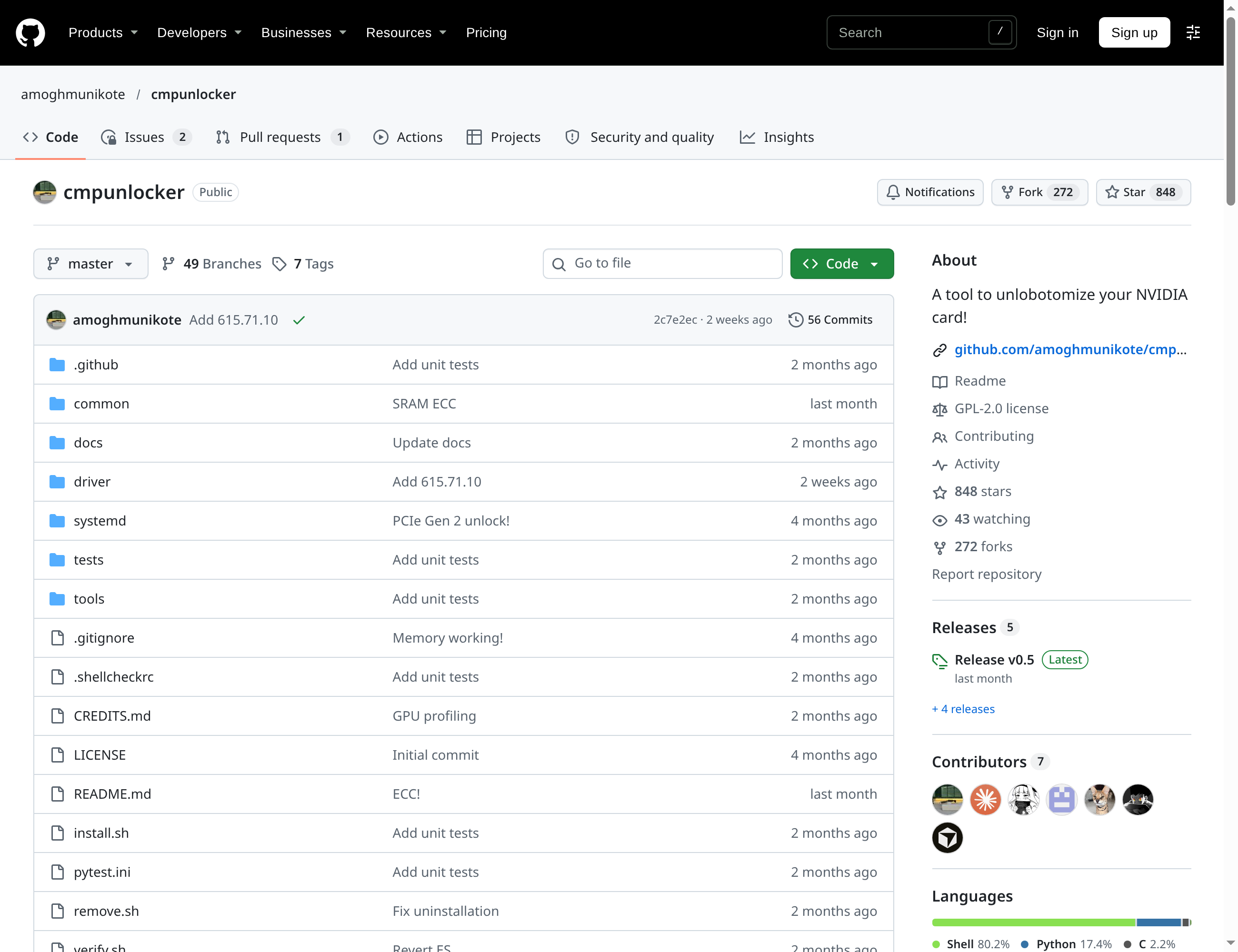
Caption: The existing tool, which predates this post by months and targets the same segmentation fuses. Screenshot: GitHub.
The line this belongs to
Fit tables everywhere, including this site’s, describe cards as Nvidia sells them. A card whose memory, compute and link width can all be renegotiated by the owner breaks that assumption, and it is happening at the bottom of the market, on hardware that was meant to be thrown away.
The honest framing: this is a research result about product segmentation, not a buying guide. The card is discontinued, the process is delicate, and the result varies by die. But it does prove something useful about what a fuse is worth, which is exactly as much as the cost of glitching it.
Discussion
Be the first to commentStart a discussion
Got a take on this, a rig to show off, or a benchmark that says otherwise? Sign up and start the thread - your comment publishes instantly once you're in.